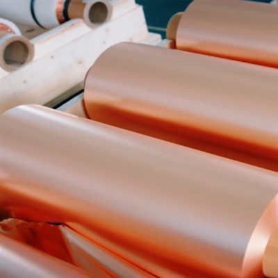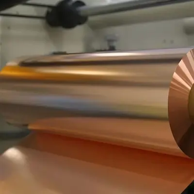


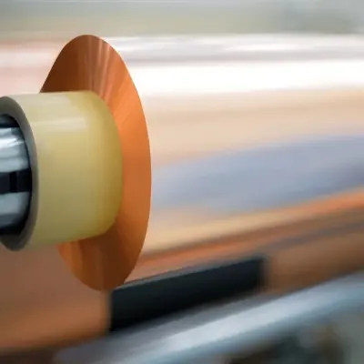
HVLP (Hyper Very Low Profile) copper foil is a specialized electrodeposited copper foil featuring an ultra-smooth surface with extremely low profile height. It is a core material for high-frequency, high-speed printed circuit boards (PCBs) in 5G/6G communication systems, AI servers, and high-performance computing infrastructure.
The fundamental physics is straightforward: at high frequencies, current in a conductor concentrates within a thin layer near the surface - the skin effect. At 56 GHz (the Nyquist frequency of 112G PAM4), the skin depth in copper is approximately 0.28 μm. When the copper surface has roughness features on the same order as this skin depth, the current path becomes longer than the geometric trace length, and the effective resistivity of the conductor increases significantly. HVLP copper foil, with its ultra-low surface roughness, addresses this challenge by minimizing conductor loss at high frequencies.
As AI accelerators and high‑speed networking equipment transition from HVLP‑2/HVLP‑3 to HVLP‑4 grade materials, demand for ultra‑low profile copper foil continues to surge. HVLP copper foil reduces signal loss by minimizing surface roughness, making it a critical material for high‑speed computing applications such as AI servers, 5G base stations, data center switches, and 800G/1.6T optical modules.
HVLP Copper Foil Grade Specifications
HSMetal supplies a full range of HVLP copper foil grades to meet diverse application requirements. Surface roughness is the primary classification criterion, with Rz (ten-point mean roughness) as the key performance indicator.
| Grade | Surface Roughness (Rz) | Typical Applications |
|---|---|---|
| HVLP-1 | 1.5–2.0 μm | Mid‑low speed PCBs, 5G small cell base stations, standard AI servers |
| HVLP-2 | 1.0–1.5 μm | Medium‑high speed communication, AI edge servers, 5G base station RF boards |
| HVLP-3 | 0.5–1.0 μm (as low as 0.87 μm) | Mid‑high end AI servers, 5G base stations, high‑speed switches, PCIe 5.0, 1.6T optical modules |
| HVLP-4 | ≤0.6 μm (Rz stable <0.52 μm, Ra 0.15–0.25 μm) | High‑end AI accelerators, 77 GHz automotive radar, satellite communications, ultra‑high‑speed data centers |
| HVLP-5+ | ≤0.5 μm (Rz 0.2–0.5 μm) | Chiplet high‑speed interconnect, terahertz communications, 224Gbps+ applications |
Available Thicknesses: 9 μm, 12 μm, 15 μm, 18 μm, 35 μm, and custom specifications. Standard product thickness range: 12–35 μm.
Key Properties
- Ultra‑low surface roughness (Rz as low as 0.2–0.5 μm for HVLP-5+)
- Significantly reduced skin effect losses at high frequencies
- Superior signal integrity for high‑speed digital transmission
- Excellent etchability for fine‑line circuit fabrication
- Good peel strength with Low‑Dk/Df resin systems
- Complies with IPC‑4562A specifications
Product Parameters
|
Item |
VLP |
HVLP |
Test Method |
||||||||
|
Thickness of copper |
9 |
12 |
15 |
18 |
35 |
9 |
12 |
15 |
18 |
IPC-TM-650 |
|
|
Area Weigth |
80±5 |
105±5 |
133±5 |
150±5 |
280±5 |
80±5 |
105±5 |
133±5 |
150±5 |
||
|
Roughness(µm) |
Shiny(Ra) |
Ra≤0.43 |
|||||||||
|
Matte(Rz) |
≤3.0 |
≤3.0 |
≤3.5 |
≤3.5 |
≤4.0 |
≤2.5 |
≤2.5 |
≤2.5 |
≤2.5 |
||
|
Peel Strength |
≥0.8 |
≥0.8 |
≥0.8 |
≥0.9 |
≥1.0 |
≥0.8 |
≥0.8 |
≥0.8 |
≥0.8 |
||
|
Tensile Strength |
R.T.(23℃) |
≥28 |
|||||||||
|
H.T.(180℃) |
≥15 |
||||||||||
|
Elongation(%) |
R.T.(23℃) |
≥4 |
≥4 |
≥5 |
≥5 |
≥6 |
≥4 |
≥4 |
≥5 |
≥5 |
|
|
H.T.(180℃) |
≥6 |
≥6 |
≥8 |
≥8 |
≥10 |
≥6 |
≥6 |
≥6 |
≥6 |
||
|
Penetrating Point/Pinhole(Piece/m²) |
Penetrating Point≤5,Pinhole=0 |
||||||||||
What is the difference between HVLP, VLP, and RTF copper foil?
These copper foil types are classified by surface roughness:
| Type | Surface Roughness (Rz) | Typical Max Frequency | Key Feature |
|---|---|---|---|
| STD (Standard) | ~5–10 μm | < 5 GHz | General purpose |
| RTF (Reverse Treated Foil) | ~3–5 μm | ~15 GHz | Lower roughness than STD |
| VLP (Very Low Profile) | ~1.5–3 μm | ~28 GHz | Low profile for high speed |
| HVLP (Hyper Very Low Profile) | ~1–2 μm | 40 GHz+ | Ultra‑low profile for ultra‑high speed |
You can think of VLP as the standard answer for thin-profile copper, while HVLP represents the best answer for pursuing ultra-low insertion loss.
Customer Case
Project Background - Korean High‑Frequency CCL Manufacturer
A leading Korean CCL manufacturer focused on AI server & 5G communication substrates contacted HSMetal for HVLP copper foil qualification and mass supply.
The customer developed new‑generation M8‑class high‑speed copper‑clad laminates targeting 112G‑224G PAM‑4 signal channels for AI accelerator boards and 800G/1.6T optical‑module PCBs.
Existing imported HVLP material faced long lead‑time, unstable batch‑to‑batch Rz consistency and high procurement costs.
Critical requirements: stable controlled Rz roughness, good resin adhesion, low high‑frequency insertion loss, full compliance with Korean PCB‑CCL industry testing standards, plus flexible small‑batch sample validation before mass‑volume delivery.
Pain point: Poor surface uniformity would directly cause signal attenuation and low PCB‑manufacturing yield for high‑frequency circuits.
Our Solution
HSMetal delivered a customized HVLP copper‑foil solution for this Korean project:
- Provided HVLP3 & HVLP4 series copper foil with tightly‑controlled Rz tolerance to match the customer's M8‑CCL formula; delivered pre‑production samples for substrate lamination, signal‑loss and peel‑strength testing.
- Strictly controlled surface‑profile uniformity to reduce high‑frequency insertion loss and guarantee stable resin‑foil bonding performance.
- Issued complete inspection documents: surface roughness report, tensile‑elongation test data and chemical‑composition certificates for Korean‑side qualification review.
- Supported phased‑delivery mode: lab sample → pilot‑lot trial → ramp‑up mass production, shortening the customer's material‑qualification cycle.
- Adjusted packaging and export documentation to fit Korea import customs requirements, ensuring on‑time shipment.
HSMetal delivered a tailored solution with our premium HVLP (Hyper Very Low Profile) Copper Foil – an ultra‑smooth, low‑profile copper foil engineered specifically for high‑frequency, high‑speed PCB applications.
| Parameter | Specification |
|---|---|
| Product | HVLP Copper Foil (Hyper Very Low Profile) |
| Surface Roughness (Rz) | From 1.5μm down to ≤0.55μm (HVLP‑1 through HVLP‑5+) |
| Thickness Range | 12–35μm (standard HVLP); ultra‑thin options available |
| Key Properties | Ultra‑low surface profile, minimized skin effect loss, excellent peel strength, high thermal reliability |
| Applications | AI servers, 5G/6G base stations, high‑speed networking, optical modules, automotive radar |
Project Outcome: The HVLP copper foil passed the customer's full qualification. It is now used for their AI‑server substrate and 5G‑RF‑module CCL production, helping shorten their supply lead‑time and lower overall material costs.
Packages and Delivery


- Ultra‑Low Surface Roughness – Surface roughness as low as Rz ≤ 0.55μm (HVLP‑5+), significantly reducing signal loss at high frequencies
- Multiple Grade Options – HVLP‑1 through HVLP‑5+ to match specific application requirements:
- HVLP‑2 (Rz 1.0‑1.5μm) – Industry standard for 5G base stations and AI servers
- HVLP‑3 (Rz ≤1.1μm) – For high‑speed computing and 112G PAM4 applications
- HVLP‑4 (Rz 0.3‑0.8μm) – For next‑generation AI accelerators and 1.6T optical modules
- HVLP‑5+ (Rz ≤0.55μm) – For 224Gbps and millimeter‑wave 5G/6G applications
- Consistent Quality – Rigorous process control ensuring batch‑to‑batch consistency
- Global Supply Chain – Reliable production capacity to support long‑term partnerships
- Competitive Lead Times – Shorter delivery windows compared to domestic alternatives
- Full Traceability – Complete material test reports (MTR) and quality documentation with every shipment
Key Product Benefits
- Minimizes skin‑effect‑related signal loss under high‑frequency working conditions
- Precise, repeatable Rz surface‑roughness control across batches
- Excellent peel‑off strength with diverse resin systems (PPO, epoxy etc.)
- Good tensile strength & elongation for PCB multi‑layer pressing processes
- Multiple grades available: HVLP1, HVLP2, HVLP3, HVLP4, HVLP5+, HVP31 (for PPO substrate), HVLPHF4
- Supports sample evaluation and export‑oriented mass‑order shipments
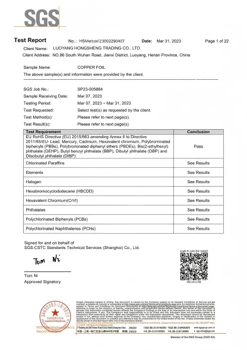
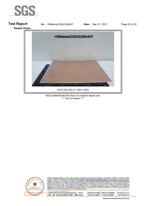
Certificate
Our Certificate


Key Applications
HSMetal HVLP copper foil is engineered for a wide range of high‑frequency and high‑speed applications:
- AI Servers & Accelerators – GB200/GB300/Rubin architecture motherboards, GPU/NPU carrier boards, OAM/UBB modules. A single AI server consumes roughly 30% more copper foil than a traditional server, with HVLP copper foil consumption per unit estimated at eight times that of conventional servers.
- 5G/6G Base Stations – RF boards, antenna systems, millimeter‑wave communication modules
- High‑Speed Networking – Data center switches (up to 3.2T), 800G/1.6T optical module PCBs, 112G/224G PAM4 SerDes backplanes
- Automotive Radar – 77 GHz millimeter‑wave radar PCBs
- Satellite Communications – High‑reliability, low‑loss RF substrates
- Advanced Packaging – FCBGA package substrates, high‑density interconnect (HDI) boards, IC carrier boards
Company Profile
HSMetal is a specialized manufacturer of high‑performance non‑ferrous metal materials, focusing on high‑end copper foil, copper‑alloy strip and special metal solutions for 5G communication, AI server, CCL and PCB industries.
With complete in‑house R&D, production and testing capabilities, we strictly control key indicators including surface roughness (Rz), peel strength and insertion‑loss performance for HVLP‑grade copper foil. Every batch is supported by full inspection reports to satisfy strict qualification requirements of overseas high‑frequency substrate manufacturers.
We have accumulated rich project experience serving customers across South Korea, Japan, Southeast Asia, Europe and North America. We offer flexible workflows from small‑sample validation, pilot production to large‑volume mass shipment, together with export‑oriented documentation and customized packaging for Korean and other international markets.
Beyond HVLP copper foil, our material portfolio also covers RTF, VLP, carrier copper foil, Cu‑Ni‑Si alloy strips and Cr‑Zr‑Cu products, to support your full‑range high‑frequency hardware material demands.
We combine stable product consistency, competitive lead‑time and responsive technical support, aiming to be your long‑term trusted supplier for high‑frequency metal‑material projects.
Our Factory

Electrodeposited Copper Foil Cleanroom Production Workshop

Quality‑control inspection for electrodeposited copper‑foil on production‑line

Automated continuous production line for HVLP Copper Foil

Comprehensive Real‑Time Monitoring of Electrolyte Additives
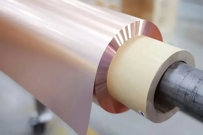
Finished jumbo roll of HVLP Copper Foil UltraLow Profile Copper Foil for High Frequency Circuits

High‑Precision Analysis of Copper Foil Microstructue
FAQ
Q1:What is HVLP copper foil?
A:HVLP stands for Hyper Very Low Profile. HVLP copper foil is a specialized electrodeposited copper foil featuring an ultra-smooth surface with extremely low profile height. It is a core material for high-frequency, high-speed printed circuit boards (PCBs) used in 5G/6G communication systems, AI servers, and high-performance computing infrastructure.
Unlike standard copper foils (HTE) with rough surfaces (Rz ≈ 5–10 μm), HVLP copper foil achieves surface roughness as low as Rz < 1.5 μm, significantly reducing high-frequency signal transmission loss caused by the skin effect.
Q2:How does HVLP copper foil reduce signal loss?
A:At high frequencies, electrical current concentrates near the conductor surface – this is known as the skin effect. The rougher the copper surface, the longer the effective current path becomes, increasing conductor loss.
HVLP copper foil, with its ultra-smooth surface, minimizes this effect. Studies show that at 25 GHz, a standard-profile foil (Rz ≈ 10 μm) adds roughly 0.8–1.2 dB/inch more loss than an HVLP foil (Rz ≈ 2 μm). HVLP-type copper foils exhibit better high-frequency transmission performance due to lower signal scattering, reflections, and surface inductance.
Q3:Is HVLP copper foil suitable for outer layers?
A:Caution is advised. Because HVLP copper foil has an ultra-smooth surface, it exhibits lower adhesion strength to prepreg materials during lamination. This can lead to delamination or blistering issues.
Recommendation: HVLP copper foil is typically recommended for inner layers where signal integrity is critical. For outer layers, RTF (Reverse Treated Foil) or other surface‑treated foils may be more appropriate from a reliability perspective. If outer‑layer HVLP is required, special surface treatment processes should be considered.
Q4:What thicknesses are available for HVLP copper foil?
HSMetal offers HVLP copper foil in standard thicknesses:
- 12 μm (1/3 oz) – For fine‑line, high‑density designs
- 18 μm (1/2 oz) – For general high‑speed applications
- 35 μm (1 oz) – For higher current‑carrying capacity
Custom thickness specifications are available upon request. All products comply with IPC‑4562A specifications.
Q5:Why is there a supply shortage of HVLP copper foil?
The rapid adoption of AI servers, 5G infrastructure, and high‑speed networking has created a structural supply gap for high‑end HVLP copper foil. Industry projections indicate:
- HVLP4 copper foil supply is projected to face a shortage exceeding 40% in 2026
- The deficit is expected to expand from 1,500 tons in 2026 to 2,500 tons in 2027
This supply concentration creates both a risk and an opportunity for qualified international suppliers like HSMetal to provide reliable, high‑quality HVLP copper foil to global customers.
Q6: What is HVLP copper foil and how is it different from regular RTF / VLP copper foil?
A: HVLP (High‑Very‑Low‑Profile) copper foil features much tighter‑controlled ultra‑low Rz surface roughness. Compared with conventional RTF or VLP foil, it greatly reduces high‑frequency signal loss caused by the skin effect, making it ideal for 112G‑224G PAM‑4, 800G/1.6T high‑speed CCL, AI server and mm‑wave 5G hardware.
Q7: What Rz grades of HVLP copper foil can you supply?
A: We provide full‑series HVLP grades: HVLP1, HVLP2, HVLP3, HVLP4, HVLP5+, HVP31 (optimized for PPO substrate), HVLPHF4. Rz ranges from Rz 1.5‑2.0 μm down to ≤1.1 μm and ultra‑low‑roughness options. Custom Rz tolerance can be adjusted according to customer's CCL formula requirements.
Q8: Can you provide samples for qualification for Korean CCL / PCB manufacturers?
A: Yes. We support lab‑scale sample supply for material qualification, followed by pilot trial lots before mass‑volume order. All samples come with full inspection reports including surface roughness, tensile‑elongation and chemical‑composition certificates to meet Korean‑side review standards.
Q9: Which resin systems does your HVLP copper foil bond well with?
A: Our HVLP foil shows reliable peel‑strength performance with mainstream resin matrices, including epoxy and PPO. HVP31 grade is specially tuned for PPO‑based high‑speed substrates.
Q10: What are your typical lead‑times for samples and bulk orders for South‑Korea shipments?
A: Sample lead‑time: 7‑10 working days. Mass‑production lead‑time depends on grade & order volume. We prepare export documents and custom‑fit packaging for Korea customs clearance to guarantee on‑time delivery. Please contact our sales team for an exact schedule.
Q11: Can HVLP copper foil be used for FCCL flexible copper‑clad laminates?
A: Selected HVLP grades are applicable for partial high‑frequency FCCL projects. Kindly share your working frequency, substrate thickness and target peel‑strength requirement; our technical team will recommend the most suitable grade.
Q12: What test reports will you provide with each batch?
A: Each shipment includes COC (Certificate of Conformity), surface‑roughness test record, tensile & elongation data and chemical composition report. Additional test documentation can be arranged upon request for customer qualification audit.
Q13: Do you offer other high‑frequency copper‑foil products besides HVLP?
A: Yes. Our portfolio also covers RTF, VLP, carrier copper foil, together with Cu‑Ni‑Si and Cu‑Cr‑Zr alloy strips. Contact us if you have multi‑material sourcing needs for your high‑speed circuit project.
Q14:How does HSMetal ensure HVLP copper foil quality?
A:HSMetal's HVLP copper foil is manufactured under strict quality control to ensure:
- Consistent surface roughness – Batch‑to‑batch Rz control within specification
- Full traceability – Complete material test reports (MTR) with every shipment
- IPC compliance – Manufactured to IPC‑4562A and international standards
- Application support – Technical guidance for material selection and PCB stack‑up optimization
Q15: What is the Minimum Order Quantity (MOQ)?
A: Normally MOQ is 200kg, We always expect more opportunities with you. But for some special material or special size let's communicate the actual status.
Q16: What payment terms do you accept?
A: We accept T/T, L/C, and other common methods. For new customers, we usually require 50% deposit and 50% balance before shipment. Flexible terms can be negotiated for long-term partners
Q17:How can I request samples or get a quotation?
Contact HSMetal today for:
- Technical datasheets and specification documents
- Sample requests for qualification testing
- Tailored quotations for your specific thickness and grade requirements
Reach Us for Sample and Quotation
Hot Tags: HVLP Copper Foil — Ultra‑Low Profile Copper Foil for High‑Frequency Circuits, ultra-low profile copper foil, 5G PCB copper foil, high-frequency copper foil, AI server copper foil, low roughness copper foil