


HSMetal, a professional Chinese manufacturer of high-performance copper nickel silicon alloy materials, has successfully completed customized production and full-qualified delivery of 4mm width C70250 Copper Nickel Silicon Strip for a local United States semiconductor manufacturer. The batch of precision alloy materials is specially applied to high-precision semiconductor lead frame contacts and electronic component stamping production.
Different from ordinary standard strips, this US project required strict flatness consistency, edge burr-free performance and stable mechanical properties for continuous high-speed stamping. Combined with the client's technical drawing standards for lead frame production, our technical team optimized the rolling tolerance, aging hardening process and precision slitting procedure. All finished 4mm width C70250 Copper Nickel Silicon Strip achieved uniform hardness, excellent bending resistance and stable electrical conductivity, fully meeting American high-end semiconductor manufacturing requirements.
The Customer's Challenge: Extreme Precision and Consistency Required
The U.S. customer, a well-known supplier to the global semiconductor industry, had previously sourced wider strips and performed in-house slitting. However, when producing narrow strips around 4mm, they encountered persistent issues: excessive burr heights, poor edge quality, width variations exceeding ±0.05mm, and unacceptable flatness (warpage). These defects caused frequent tool wear, unplanned downtime, and increased scrap rates on their high-speed stamping lines.
The customer urgently needed a supplier capable of delivering ready-to-stamp 4.0mm ± 0.02mm strips with superior edge finish, consistent mechanical properties, and full traceability – all while meeting the stringent cleanliness and surface requirements for IC lead frame applications.
Our Solution: Full-Process Quality Control and Precision Slitting Technology
Our technical team conducted a thorough online consultation with the customer to define the critical parameters:
| Parameter | Requirement |
|---|---|
| Width | 4.0mm ± 0.02mm |
| Burr Height | ≤ 0.02mm (compatible with die clearance) |
| Flatness (warpage) | ≤ 0.5mm per 100mm width (SEMI standard) |
| Temper | TM04 (Full‑Hard) |
| Tensile Strength | 760 – 850 MPa |
| Yield Strength (Rp0.2) | ≥ 720 MPa |
| Hardness | 220 – 270 HV |
| Coil Weight | 500 kg per coil (for automated feeding) |
| Edge Finish |
Deburred and radiused to prevent die scratching |
To meet these specifications, we deployed our multi-roll precision slitting line equipped with laser-based in-line width measurement and automatic edge deburring stations. Each slit strand was individually inspected for width, burr height, and surface roughness. We also applied a light anti-oxidation oil film and protected the coils with VCI paper and moisture-proof packaging to ensure pristine condition upon arrival.
In addition, we provided the customer with comprehensive Mill Test Certificates (MTC) , dimensional inspection reports, tensile and hardness test results, and surface roughness analysis – all traceable to the original melt heat number.
Proven Results: Expanded Partnership
During the whole production process, HSMetal implemented strict full-process quality control. Each coil was strictly inspected in terms of chemical composition, dimensional tolerance, surface quality, tensile strength and stress relaxation performance. The entire batch passed factory inspection and was delivered with complete MTC certification and full inspection reports, helping the US client complete incoming quality verification smoothly.
This successful US delivery further proves HSMetal's mature customization and export capability for high-end C70250 semiconductor-grade copper strips. We are capable of stably supplying standard and custom-width Cu-Ni-Si alloy strips with flexible specifications, supporting both sample trial orders and large-scale mass production for global semiconductor, automotive electronics and new energy industries.
Product Production Process
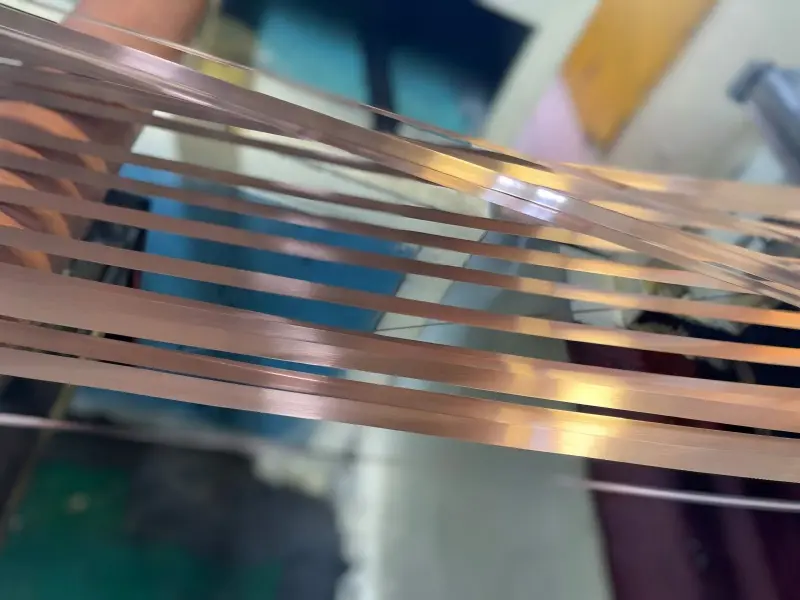
C70250 Copper Nickel Silicon Strip Slitting In Production Line
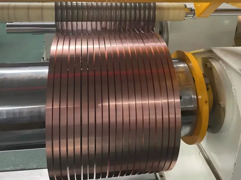
C70250 Copper Nickel Silicon Strip Slitting Into Narrow Width
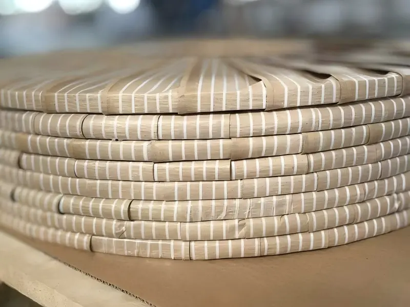
Packages
Our Commitment and Broader Capabilities
While this case study highlights the 4.0mm width, our precision slitting technology is capable of processing widths as narrow as 1.0mm (and above), with thicknesses ranging from 0.05mm to 3.0mm. We supply C70250 in multiple tempers (TM00, TM02, TM03) and can tailor dimensions, edge profiles, and packaging to meet any customer specification.
Beyond lead frames, our C70250 strip is widely used in:
- 5G communication connectors
- Automotive terminals and busbars
- Relay springs and contact components
- Type-C and other high-end electrical connectors
- Aerospace and defense applications
We invite semiconductor, electronics, and automotive manufacturers worldwide to explore how our precision-slitting expertise and vertically integrated production can support your high-reliability applications.
For technical inquiries, samples, or a personalized quotation, please contact our sales team.
Pls view our proudct C70250 Copper Nickel Silicon Strip for Lead Frame Semiconductor for more details
FAQ
Q1: What is the minimum slitting width you can offer?
A: We can slit down to 1.0 mm with tight tolerances. For high‑volume stamping, we often recommend optimized widths (e.g., 4.0 mm) to balance productivity and material yield – we customize based on your die layout.
Q2: Why choose TM04 over other tempers?
A: TM04 provides the highest strength (≥760 MPa) and best stress relaxation resistance, making it ideal for applications with high mechanical loads and elevated temperatures. However, it has lower formability (elongation ≥2%). If your part requires tight bending or complex forming, consider TM03 or TM02 – we can advise based on your drawing.
Q3: How do you control flatness and warpage?
A: We use multi‑roll leveling and tension‑leveling, achieving flatness ≤ 0.5 mm per 100 mm width (SEMI standard). Additional stress‑relief annealing can be applied for critical stamping processes.
Q4: Do you offer trial samples? What is the MOQ?
A: Yes. Standard MOQ is 500 kg, but we accept sample orders of 100‑200 kg for customer qualification.
Q5: What surface protection do you provide?
A: We apply a light anti‑oxidation oil film, or offer dry/oil‑free surfaces and VCI paper interleaving upon request. All coils are vacuum‑sealed and packed in fumigated wooden cases.
Q6: Can you provide third‑party inspection?
A: Yes, we can arrange SGS, BV, or other inspections at your cost. We also supply our own MTC (EN 10204 Type 3.1) with full chemical, mechanical, and dimensional data.
Q7: What are the typical aging conditions for TM04 after stamping?
A: TM04 is already in the fully hardened state. Post‑stamping aging is usually not required, but if additional precipitation hardening is desired, temperatures of 350‑450°C for 2‑4 hours can be applied – please consult our technical team.
Q8: How do you ensure batch‑to‑batch consistency?
A: We use SPC throughout the production chain – from melt to final slitting. Every coil has a unique heat number for full traceability.
Q9: What is your export packaging?
A: See the commercial terms table below. We use VCI paper, plastic film, edge protectors, and heavy‑duty wooden pallets/crates suitable for long ocean freight.
Q10: Can I customize thickness, width, and temper?
A: Yes. We offer thickness 0.05‑3.0 mm, width ≥1.0 mm, and any temper (TM00 to TM04). Custom combinations may require a higher MOQ – please inquire.


