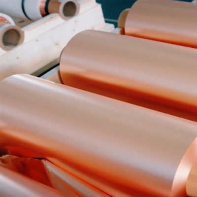
How you use this product: This RTF3 Reverse‑Treated (RTF) copper foil is applied as inner‑layer signal conductor when laminating with low‑loss CCL substrates. It is designed for fabricating multilayer high‑speed PCBs for AI servers, high‑speed switches, storage hardware and 5G communication equipment. The treated side bonds with dielectric material; the ultra‑smooth surface faces signal traces, suppressing high‑frequency signal loss caused by skin‑effect. It supports PCIe Gen5 platforms including Intel Eagle Stream and AMD Genoa, and can serve as a high‑performance alternative to TDK‑grade RTF copper foil for your high‑end PCB projects.
As global hyperscale data centers roll out PCIe Gen5 and next‑gen computing hardware, PCB manufacturers are facing a tough trade‑off: lower surface roughness cuts signal loss, yet usually sacrifices peel strength against dielectric substrates. Our self‑developed High‑Speed RTF3 RTF copper foil solves this core pain point, delivering balanced low roughness, reliable bonding force, high‑temperature dimensional stability and fine‑line etching performance. Developed and mass‑produced by our China factory, it matches the performance benchmark of mainstream high‑end RTF material, helping CCL and PCB manufacturers meet strict requirements from AI computing and telecommunication clients without relying fully on imported supplies.
Key Performance Data (1oz RTF3 Copper Foil)
| Item | Typical Value | Value to Your Business |
|---|---|---|
| Treated‑side Roughness (Rz) | 1.85 μm (≤2.1 μm Max) | Greatly reduces high‑frequency conductor loss, ensures signal integrity for PCIe Gen5 high‑speed lanes |
| Peel Strength on Low‑loss Material | 4.8 lb/in | Maintains strong substrate adhesion even at ultra‑low roughness, avoids delamination risk |
| Microstructure | Columnar grain preserved after annealing | Anti‑deformation under PCB thermal processing; less board warpage, higher finished‑product yield |
| Anti‑Side‑Etching Performance | Verified by end‑user trials | Produces sharp, intact fine traces for HDI & high‑density inner‑layer circuits |
Positioning note: RTF3 is the smoothest grade in the RTF family (RTF1 ≤3.0 μm, RTF2 ≤2.3 μm, RTF3 ≤2.1 μm). If your data rate is 10–25 Gbps and you need fine lines with controlled impedance, RTF3 is the right grade. Above 25 Gbps, consider VLP or HVLP.
For projects weighing copper foil options, see our full comparison of [HTE vs RTF vs VLP vs HVLP Copper Foil] to confirm which grade fits your signal‑loss, peel‑strength and cost targets.
If you are confused between electrolytic and rolled‑annealed copper for your PCB stack‑up, check [ED Copper Foil vs RA Copper Foil: A Buyer's Guide to Selection and Risk Avoidance] to sort out material differences and common procurement risks.
Core R&D & Technical Strength
We combine precision cathode roller polishing and proprietary special roughening treatment processes to control treated‑side surface roughness down to typical Rz 1.85 μm (max ≤2.1 μm). Under high‑frequency conditions, high‑speed signals travel along conductor surface due to skin‑effect; our ultra‑flat surface reduces signal path turbulence and minimizes insertion loss for high‑speed serial links.
Our exclusive additive formula locks stable columnar grain structure even after PCB lamination and soldering thermal cycles. Unlike conventional copper foil whose grains slip and deform under heat, RTF3 retains mechanical strength at elevated temperature, effectively preventing board warpage and delivering outstanding dimensional stability for finished laminates.
For HDI fine‑circuit manufacturing, micro‑crystal copper modification suppresses undercut during etching. Your production team can obtain complete, clean fine traces and avoid yield loss caused by excessive side‑etching.
Where RTF Copper Foil Is Used
AI servers and high-speed computing platforms
PCIe Gen5 server platforms (Intel Eagle Stream, AMD Genoa), AI training and inference servers, high-speed backplanes. These designs run 10–25 Gbps per lane and require low loss with reliable multilayer lamination.
High-speed switches and storage devices
800G and 400G switches, data center storage arrays. RTF's low roughness keeps insertion loss within budget while its peel strength supports multiple lamination cycles.
5G base stations and communication equipment
5G infrastructure, high-end routers, mmWave front-end boards. RTF3 balances loss and cost for 10–25 Gbps signal layers.
HDI and fine-line PCB
Advanced HDI boards with 50 μm and below line widths. RTF's differential two-side treatment gives better etching control than HTE, reducing side-etching and improving yield.
Automotive high-speed electronics
Automotive radar, in-vehicle high-speed gateways, autonomous driving domain controllers. RTF provides the thermal and dimensional stability these applications require.
How to Choose: RTF vs HTE vs VLP/HVLP
| Your Data Rate / Need | Recommended Foil | Why |
|---|---|---|
| ≤10 Gbps, power/ground layers | HTE | Cost-effective, excellent thermal reliability |
| 10–25 Gbps, signal layers | RTF3 | Low loss, fine-line etching, reliable peel strength |
| 25 Gbps+, AI/data center, M8/M9 | HVLP | Ultimate low loss, requires nano-roughening |
| Fine line ≤50 μm | RTF3 or HVLP | Better etching control than HTE |
| Extreme low loss, cost no object | HVLP | Rz ≤2.0 μm, down to ≤0.6 μm |
RTF3 is the balance point: smoother than HTE, more affordable than HVLP, and designed for the 10–25 Gbps range where most AI server and high-speed switch signal layers operate.
Process Notes for PCB Fabrication
Lamination and adhesion.
For 10–25 Gbps applications, plasma treatment is recommended to improve bonding on the smooth side. Confirm compatibility with your PP/resin system before production.
Etching and fine lines.
RTF's two-side differential treatment gives better etching control than HTE. Customer-verified: complete lines, no side-etching, suitable for HDI and fine-line processes at 50 μm and below.
Reliability verification.
Perform cross-hatch testing per ISO 2409. For high-reliability applications, run thermal cycling and reflow testing to confirm dimensional stability and peel strength after multiple cycles.
Market‑Driven Benefits for Buyers
- Match latest hardware trends: Specially engineered for AI server, high‑speed switch, data‑center backplane and 5G base‑station inner‑layer PCB, fits Intel Eagle Stream, AMD Genoa PCIe Gen5 new‑generation platforms.
- Reduce your supply‑chain risk: High‑performance domestic alternative to imported grades such as TDK RTF copper foil. Sample validation, mass‑supply capacity and flexible MOQ support your project ramp‑up.
- Boost your production yield: Balanced low‑roughness & high peel strength; stable high‑temperature property; superior fine‑line etching capability. Less board reject from warpage, delamination or trace distortion.
- Optimize total cost: Avoid over‑paying for premium imported materials while keeping the high‑frequency performance your customers demand. We support custom width & technical collaboration for new‑material joint‑development.
Commercial and Delivery Term
| MOQ | 200kg |
| Lead Time | 15‑20 working days after receiving deposit, depends on raw material status & order volume |
| Payment Term | 30% T/T deposit against PO confirmation; 70% balance against copy of Bill of Lading• Long‑term strategic clients: negotiable payment terms available |
| Available Price Terms | EXW, FOB, CIF, DAP |
| FOB Port | Shanghai / Ningbo (other Chinese ports upon request) |
| Custom Service | Custom slitting width; dedicated batch test report; special export packaging; joint substrate‑matching test with customer's low‑loss prepreg / CCL |
| Packing Standard | Vacuum‑sealed packaging with desiccant, anti‑moisture carton + wooden pallet. Anti‑oxidation & anti‑damage for sea / air transit |
| Shipping Option | Sea freight, air freight; international courier for small samples; buyer‑appointed forwarder is acceptable |
| Quotation Validity | 10 days. Subject to change under dramatic raw‑material price fluctuation |
About Us
We are a professional Chinese manufacturer specialized in high‑end electronic copper foil for high‑frequency & high‑speed PCB and CCL industry. Focusing on advanced copper‑foil material R&D, production and technical service, we devote ourselves to developing domestic alternative materials for AI computing, data center, 5G telecommunication and high‑end HDI circuit board markets.
Our core product portfolio covers reverse‑treated foil (RTF), ultra‑low profile copper foil and other high‑speed electrolytic copper foil grades. Equipped with complete material lab and pilot production line, our engineering team carries out formula optimization, microstructure control and application verification to balance low surface roughness, high peel strength and thermal stability. Our RTF‑3 copper foil is fully validated by multiple CCL & PCB customers for PCIe Gen5 AI server inner‑layer application.
We do not only supply copper foil rolls. We provide full‑cycle technical support including sample qualification, substrate matching test, manufacturing‑process consultation and after‑sales problem‑solving. Our goal is to help global PCB and CCL customers mitigate supply‑chain risks, shorten material‑qualification cycle and achieve stable mass‑production with cost‑competitive high‑performance Chinese‑made copper foil.
We welcome OEM & technical co‑development projects from worldwide partners.
Our Factory

Automated continuous production line for Copper Foil

Finished Jumbo Roll of Copper Foil

Copper Foil Clean‑room Production Workshop

Comprehensive Real‑Time Monitoring of Electrolyte Additives

Quality Control Inspection For Electrodeposited Copper Foil On Production Line

High‑Precision Analysis of Copper Foil Microstructue
Q1: What is RTF copper foil used for?
A: RTF (Reverse Treated Foil) copper foil is used for high-speed PCB signal layers, especially where low conductor loss and reliable peel strength are both required. Typical applications include AI servers (PCIe Gen5 platforms such as Intel Eagle Stream and AMD Genoa), high-speed switches, data center storage devices, 5G base stations, high-speed backplanes, and HDI fine-line boards.
Q2: Can your RTF‑3 replace imported high‑end RTF copper foil? What is the key benchmark?
A: Yes. Typical treated‑side Rz 1.85μm (max ≤2.1μm) and peel strength 4.8 lb/in on low‑loss substrate are comparable with mainstream imported high‑speed RTF grades. We strongly suggest customers complete sample evaluation together with your own low‑loss prepreg for full qualification before mass production.
Q3: What thickness / ounce do you supply for RTF‑3?
A3: RTF‑3 main grade is 1oz (35μm). Other thickness options can be discussed according to your project requirement. Custom slitting width is supported.
Q4: How about its high‑temperature performance? Will my PCB board warp after pressing?
A: RTF‑3 keeps columnar grain structure after high‑temperature annealing. It restrains lattice slip under PCB lamination and reflow thermal cycles, delivering good dimensional stability. It effectively reduces board‑warpage risk compared with ordinary electrolytic copper foil. Actual performance is related to your full stack‑up and pressing profile.
Q5: Does RTF‑3 work well for fine‑line / HDI etching process? Any side‑etch concern?
A: Our micro‑crystallization treatment improves etching performance and suppresses side‑etching. Multiple customer production tests prove clean and complete fine traces. You may adjust your etching parameter according to your existing process condition.
Q6: What documents can you provide for qualification?
A: We can provide material datasheet, batch inspection test report, MSDS, export documents. We also support joint substrate‑matching test upon request.
Q7: What is your sample and bulk‑order lead‑time? Can you accept small trial order?
A: Sample lead‑time: 7‑10 working days. Bulk order lead‑time: 15‑20 working days after deposit. Small trial‑batch order is acceptable for new‑product qualification. MOQ is negotiable.
Q8: What if oxidation or surface defect occurs after goods arrival?
A: Please inspect goods immediately once receiving. Keep original vacuum‑sealed packaging. If quality issue caused by our production & packing, please provide photos & test evidence within agreed time; we will work out solution including replacement or compensation according to contract terms. Improper storage and transportation by buyer is excluded.
Q9: What does "reverse treated" mean?
A: In standard ED copper foil (like HTE), the rough matte side bonds to the substrate, and the smooth side faces the signal path. In RTF, the process is reversed: the smooth (drum) side is treated for bonding to the substrate, while the micro-roughened side carries the signal. This gives you a smoother signal path (lower loss) while keeping enough adhesion for multilayer lamination.
Q10: What is the roughness of HSMetal RTF3 copper foil?
A: The treated-side roughness is Rz ≤2.1 μm, with a typical value of 1.85 μm on 1 oz foil. This reaches a very low profile level, effectively reducing skin-effect loss at high frequency. Roughness is verified per batch, not just quoted as a datasheet number.
Q11: What peel strength does RTF3 provide?
A: HSMetal RTF3 provides 4.8 lb/in typical peel strength. This is important because low roughness usually means weaker adhesion - RTF3 maintains both low roughness and strong peel strength, making it usable in high-volume multilayer production.
Q12: Why does RTF need plasma treatment?
A: RTF bonds its smooth side to the substrate. That smooth surface has less mechanical anchoring than HTE's rough matte side. For 10–25 Gbps applications, plasma treatment is recommended to improve bonding and prevent delamination during lamination. Confirm compatibility with your PP/resin system before production.
Q13: What data rate is RTF3 suitable for?
A: RTF3 is designed for the 10–25 Gbps range. This covers most AI server signal layers, high-speed switches, 5G infrastructure, and data center equipment. For ≤10 Gbps, HTE is more cost-effective. For 25 Gbps+, VLP or HVLP is required.
Q14: Can RTF3 handle fine-line etching?
A: Yes. RTF's two-side differential treatment gives better etching control than HTE. Customer-verified results show complete lines after etching, no side-etching, suitable for HDI and fine-line processes at 50 μm and below. HTE, by contrast, is stable only at line widths ≥75 μm.
Q15: Why does high-temperature dimensional stability matter?
A: PCB lamination and soldering expose the foil to high temperature. Ordinary copper foil grains tend to relax and change dimension, which can warp the board. HSMetal RTF3 uses a special additive formulation that maintains columnar grain structure after annealing and suppresses lattice slip, so strength does not degrade significantly at high temperature. This ensures dimensional stability of the copper-clad laminate.
Q16: Is RTF3 a direct substitute for mainstream high-speed foils?
A: HSMetal RTF3 is designed for the same application scenarios as the high-speed RTF products used on Intel Eagle Stream and AMD Genoa platforms, high-speed switches, and data center equipment. You can qualify it against your existing stack-up. For a full comparison of RTF, HTE, VLP, and HVLP, see our [HTE vs RTF vs VLP/HVLP copper foil selection guide].
Q17: What is the difference between RTF and HTE?
A: HTE is a traditional ED foil with a rough matte side bonding to resin - excellent peel strength and thermal reliability, but higher conductor loss at high frequency (Rz 4–6.5 μm). RTF reverses the treatment, putting the smooth side against the substrate and micro-roughening the signal side - lower loss, better fine-line etching, at a higher cost. ≤10 Gbps: HTE. 10–25 Gbps: RTF3.
Q18: Can RTF replace HVLP to save cost?
A: Not for 25 Gbps+ designs. RTF3 is ≤2.1 μm; HVLP is ≤2.0 μm, down to ≤0.6 μm. They are not in the same class. For 25 Gbps+ and M8/M9 materials, RTF may not meet the loss budget. Check the actual Rz requirement against your insertion loss target before substituting. See the full [PCB copper foil selection and pitfall guide].
Q19: What reliability tests should I run for RTF3?
A: Perform cross-hatch testing per ISO 2409. For high-reliability applications, run thermal cycling and reflow testing to confirm dimensional stability and peel strength after multiple cycles. If your board uses a high-Tg or low-loss resin system, confirm compatibility with the foil before production.
Q20: What is the one-line rule for choosing RTF?
A: 10–25 Gbps, fine lines, reliable peel strength → RTF3. Below 10 Gbps, HTE is more cost-effective. Above 25 Gbps, move to VLP or HVLP. RTF3 is the balance point between loss, etching, and cost.
Hot Tags: RTF Copper Foil | Reverse Treated Foil for AI Server, 5G & High-Speed PCB Signal Layers, China Factory, Reverse‑Treated Foil, RTF‑3 copper foil, high‑speed PCB copper foil, low roughness copper foil, AI server PCB copper foil, PCIe Gen5 copper foil, inner‑layer CCL copper foil