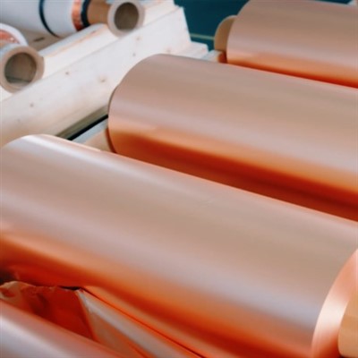
When data rates increase and signal frequencies rise, copper foil surface characteristics become increasingly important to PCB performance. Conventional copper foil with a rougher bonding surface can increase the effective current path and contribute to conductor loss, making surface profile an important consideration in high-frequency and high-speed circuit design.
HSMetal HVLP High Frequency and High Speed Copper Foil is developed for advanced electronic materials that require a controlled ultra-low-profile copper surface, reliable resin bonding, and stable mechanical properties. Produced using an independently developed additive process, this HVLP copper foil features a fine, uniform copper grain structure and a customizable low-profile surface.
With thickness options from 7 μm to 70 μm, two surface roughness grades, and controlled tensile strength, elongation, and peel strength, the product can be evaluated for high-frequency copper-clad laminates (CCL), IC packaging carrier boards, and high-density interconnection (HDI) boards.
Whether you are developing high-speed communication equipment, advanced package substrates, or high-density PCB designs, selecting the right HVLP copper foil involves more than choosing the lowest roughness value. Thickness, resin compatibility, peel strength, thermal processing, and signal integrity must all be considered together.
👉 Explore HVLP Copper Foil Specifications & Request a Sample
Typical Properties Of HVLP High Frequency and High Speed Copper Foil
| Test Item | Unit | 7 μm | 9 μm | 12 μm | 18 μm | 35 μm | 70 μm |
| Unit Area Weight | g/m² | 62±2 | 80±2 | 107±3 | 153±4 | 285±8 | 610±10 |
| Tensile Strength (Normal) | MPa | ≥300 | ≥300 | ≥300 | ≥300 | ≥300 | ≥300 |
| Tensile Strength (180°C) | MPa | ≥190 | ≥190 | ≥190 | ≥190 | ≥190 | ≥190 |
| Elongation (Normal) | % | ≥8 | ≥10 | ≥11 | ≥13 | ≥16 | ≥16 |
| Elongation (180°C) | % | ≥8 | ≥10 | ≥11 | ≥13 | ≥16 | ≥16 |
| Roughness Rz HVLP-1 treated side | μm | >1.5μm and <2.0μm | |||||
| Roughness Rz HVLP-2 treated side | μm | >1.0μm and <1.5μm | |||||
| Peel Strength (Normal) | N/mm | ≥3.5 | ≥3.5 | ≥3.5 | ≥4.0 | ≥4.0 | ≥4.0 |
| Peel Strength (288°C) | N/mm | ≥3.0 | ≥3.0 | ≥3.0 | ≥3.5 | ≥3.5 | ≥3.5 |
| Anti-oxidation (200°C/60min) | - | Non-oxidation after 200℃,60min | |||||
Note: All above tests follow IPC-TM-650 standards. The peel strength test adopts semi-cured laminate of NOUYA NPG-170D, M4 grade substrate. The values shown are typical data only and not guaranteed values.
What Is HVLP High Frequency and High Speed Copper Foil?
HVLP (Hyper Very Low Profile) High-Frequency and High-Speed Copper Foil is an ultra-low-profile material engineered for advanced electronics that demand flawless high-speed data processing. Manufactured using an advanced additive process, it features a fine, equiaxed copper grain structure, strictly controlled surface roughness, high tensile strength, and excellent elongation. Available in thicknesses from 7 μm to 70 μm, the foil delivers outstanding solderability, uniform fine nodules, and zero copper powder transfer. By significantly minimizing high-frequency signal loss caused by the skin effect, it ensures stable signal integrity, making it the ideal choice for high-speed copper-clad laminates (CCL), IC package substrates, and HDI circuits.

HVLP vs. Other Copper Foil Types: Which One Should You Choose?
Different copper foil types are designed for different manufacturing and electrical requirements. HVLP is not a universal replacement for standard ED, RTF, VLP, or rolled annealed copper foil.
| Copper foil type | Main surface or structural characteristic | Typical application direction | Key selection consideration |
|---|---|---|---|
| Standard ED / HTE copper foil | Conventional electrodeposited foil with a relatively higher surface profile | General rigid PCB and standard CCL | Cost, adhesion, and general PCB requirements |
| RTF copper foil | Reverse-treated surface designed to support bonding and circuit fabrication | Fine-line PCB and selected high-speed applications | Treatment side, etching, and adhesion |
| VLP copper foil | Very low-profile surface | High-speed PCB and lower-loss circuit materials | Surface roughness and resin compatibility |
| HVLP copper foil | Hyper very low-profile treated surface | High-frequency and high-speed PCB, advanced CCL | Low roughness balanced with peel strength |
| RA rolled copper foil | Rolled copper structure with high ductility and smooth surfaces | FPC and dynamic bending applications | Flexibility, fatigue resistance, and bending life |
Strategic Advice: Use our High-Speed RTF Copper Foil for inner-layer signal routing to save costs, and reserve HVLP for the outermost high-frequency layers. For general applications where loss is not critical, standard ED Copper Foil remains the most economical choice.
👉 Send your specification for a quotation
Our Product Advantages

Equiaxed Crystal Structure (Core Technology)
- Unlike standard foils that use columnar crystals, our HVLP foil uses an advanced additive process to form an equiaxed (spherical) crystal structure. This eliminates the risk of copper particle transfer to the dielectric, preventing costly electrical shorts and improving yield.
Extreme Thermal Reliability
- Even after thermal stress at 288°C, our peel strength remains at ≥3.0 to ≥3.5 N/mm. The tensile strength at 180°C stays above 190 MPa, ensuring your multi-layer boards won't delaminate or warp.
Ready for Laser Drilling & HDI
- The ultra-smooth S-side and uniform M-side are optimized for fine-line etching and laser drilling, making it ideal for HDI (High-Density Interconnect) and IC substrate manufacturing.
Customization & Fast Delivery
- Thickness: 7 μm to 70 μm (Custom widths available).
- Capacity: A massive 20,000-ton annual capacity guarantees stable, on-time delivery for your mass production.
Applications of HVLP High-Frequency and High-Speed Copper Foil
HVLP copper foil is essential where surface profile and signal integrity must work together. The optimal grade depends on your specific circuit design and laminate system.
| Application Field | Key Focus / Pain Points | Buyer Selection Considerations |
|---|---|---|
| 1. High-Frequency CCL | High-speed transmission & low-loss materials. | Must match low-loss resins (PTFE, PPO/PPE, hydrocarbon). Confirm target frequency, peel strength, and thermal reliability. (For extreme low-loss, evaluate HVLP-2). |
| 2. IC Packaging Substrates | Fine circuit formation & advanced packaging. | Requires ultra-low profile for fine-line etching. Verify copper-resin bonding, dimensional stability, and multilayer lamination compatibility. |
| 3. HDI Boards | High-density routing & microvias. | Balance ultra-low roughness with etching capability and bonding strength for fine line widths/spacing. |
| 4. 5G & RF Communication | Low-loss signal transmission in RF circuits. | Select the HVLP grade based on operating frequency, laminate material, and electrical targets. |
| 5. AI Servers & Networking | Controlling conductor loss for 800G/1.6T systems. | Do not select based solely on application name. Confirm the specific HVLP generation (HVLP-1 or HVLP-2) with your CCL manufacturer. |
About Us
At HSMetal, we engineer the materials that power the AI and 5G revolution. As a leading manufacturer of ultra-low-profile copper foils, we combine advanced additive technologies with strict quality control to deliver premium HVLP High-Frequency and High-Speed Copper Foil. Featuring an innovative equiaxed crystal structure, our foil guarantees zero copper powder transfer, ultra-low roughness (Rz < 1.5 μm for HVLP-2), and exceptional peel strength under extreme thermal stress (288°C). Backed by a 20,000-ton annual capacity, we support global CCL and PCB manufacturers with mass-production-ready solutions, custom specifications, and fast sampling for signal integrity validation.
Contact our technical team today to discuss your next-generation high-speed design and request a quote.

Electrolytic Copper Foil

Microporous Copper Foil

Rolled Copper Foil

Electrochemical Data Analysis

Lab Testing For Copper Foil Performance

Precision Inspection of Copper Foil
Request a Quote for HVLP High Frequency and High Speed Copper Foil
Looking for a suitable HVLP Copper Foil Supplier for high-frequency CCL, high-speed PCB, IC packaging carrier boards, or HDI applications?
Send us your requirements today:
- Thickness (7 μm – 70 μm)
- Profile Grade (HVLP-1 or HVLP-2)
- Width and roll dimensions
- Application (AI Server, 5G, HDI, IC Substrate, etc.)
Our team will review your design and provide the right HVLP specification, sample availability, and a fast quotation.
FAQ
Q1: What is HVLP high frequency and high speed copper foil?
A: HVLP stands for Hyper Very Low Profile. It is an ultra-low-profile copper foil used in high-frequency and high-speed PCB applications. Its controlled surface roughness helps reduce roughness-related conductor loss while maintaining the bonding and mechanical properties required for PCB manufacturing.
Q2: What is the difference between HVLP and VLP copper foil?
A: Both HVLP and VLP copper foils feature low-profile surfaces. HVLP generally refers to a more demanding ultra-low-profile category for high-speed and high-frequency applications. However, grade definitions vary among suppliers, so buyers should compare actual Rz values, test methods, and peel strength rather than relying only on the grade name.
Q3: What thicknesses are available for this HVLP copper foil?
A: According to the supplied product specification, available thicknesses are 7 μm, 9 μm, 12 μm, 18 μm, 35 μm, and 70 μm. Final availability and tolerances should be confirmed when requesting a quotation.
Q4: How does your HVLP foil survive high-temperature PCB assembly?
A: We use a high-performance anti-oxidation treatment. Even at 200°C for 60 minutes, the foil shows no discoloration. Furthermore, our peel strength remains above 3.0 N/mm after exposure to 288°C, ensuring the copper will not delaminate during multiple reflow cycles.
Q5: Why is surface roughness important for high-frequency copper foil?
A: At high frequencies, current concentrates near the conductor surface due to the skin effect. Surface roughness can influence the effective current path and contribute to conductor loss. A lower-profile copper surface can help reduce roughness-related loss and support signal integrity.
Q6: Does lower surface roughness always mean better HVLP copper foil?
A: No. Lower roughness can benefit high-frequency signal transmission, but it may also make resin-to-copper bonding more challenging. The best copper foil should balance surface profile, peel strength, resin compatibility, and manufacturing reliability.
Q7: Which HVLP copper foil should I choose for high-frequency CCL?
A: Start with the operating frequency, signal-loss target, resin system, and laminate manufacturer's requirements. Compare WW-HVLP-1 and WW-HVLP-2 using their actual Rz values and peel strength results. Conducting a laminate compatibility test is recommended before mass production.
Q8: Can HVLP copper foil be used for IC packaging carrier boards?
A: HVLP copper foil can be evaluated for IC packaging carrier board applications where controlled surface characteristics, circuit formation, and resin bonding are required. The appropriate thickness and surface grade depend on the package design and substrate manufacturing process.
Q9: Is HVLP copper foil suitable for HDI boards?
A: Yes, it can be considered for HDI applications requiring controlled surface roughness and suitable bonding performance. Buyers should also evaluate copper thickness, fine-line etching, resin compatibility, and multilayer lamination conditions.
Q10: What is the peel strength of this HVLP copper foil?
A: The supplied specification lists normal-condition peel strength of at least 3.5 lb/in for 7–12 μm foil and at least 4.0 lb/in for 18–70 μm foil. At 288°C, the listed values are at least 3.0 lb/in and 3.5 lb/in, respectively. The 288°C values are based on a specified M4 semi-cured substrate reference and are not guaranteed values. Actual peel strength must be confirmed using the customer's laminate system and agreed test conditions.
Q11: Can HVLP copper foil withstand high-temperature processing?
A: The supplied product data reports tensile strength and elongation values at 180°C, as well as a 200°C for 60-minute oxidation test with a non-oxidation result. Buyers should confirm whether these conditions match their actual thermal process and qualification requirements.
Q12: What is the difference between HVLP and RA rolled copper foil?
A: HVLP is commonly used for high-speed rigid PCB and advanced substrate applications where low surface profile is important. RA rolled copper foil is valued for its ductility and bending performance, making it suitable for flexible printed circuits and dynamic bending applications.
Q13: Can I use HVLP foil for inner layers?
A: Yes, but it is most cost-effective to use it for outer layers or high-frequency signal layers where insertion loss is most critical. For inner layers, our High-Speed RTF Copper Foil offers an excellent balance of low loss and cost-effectiveness.
Q14: Is HVLP suitable for laser drilling?
A: Yes. The fine, uniform grain structure and ultra-low profile make HVLP copper foil highly suitable for laser drilling in HDI and IC substrate applications.
Q15: What is your lead time for custom HVLP copper foil and What's your MOQ?
A: Standard stocked HVLP rolls can be ready within 3–7 working days. Custom formula and special surface treatment will take 15–25 working days, we will confirm the exact schedule before deposit. MOQ is 200kg.
Hot Tags: HVLP copper foil, high frequency copper foil, high speed copper foil, ultra low profile copper foil,HDI copper foil, copper foil for AI server, low loss PCB copper foil